 Phyduino Board Support
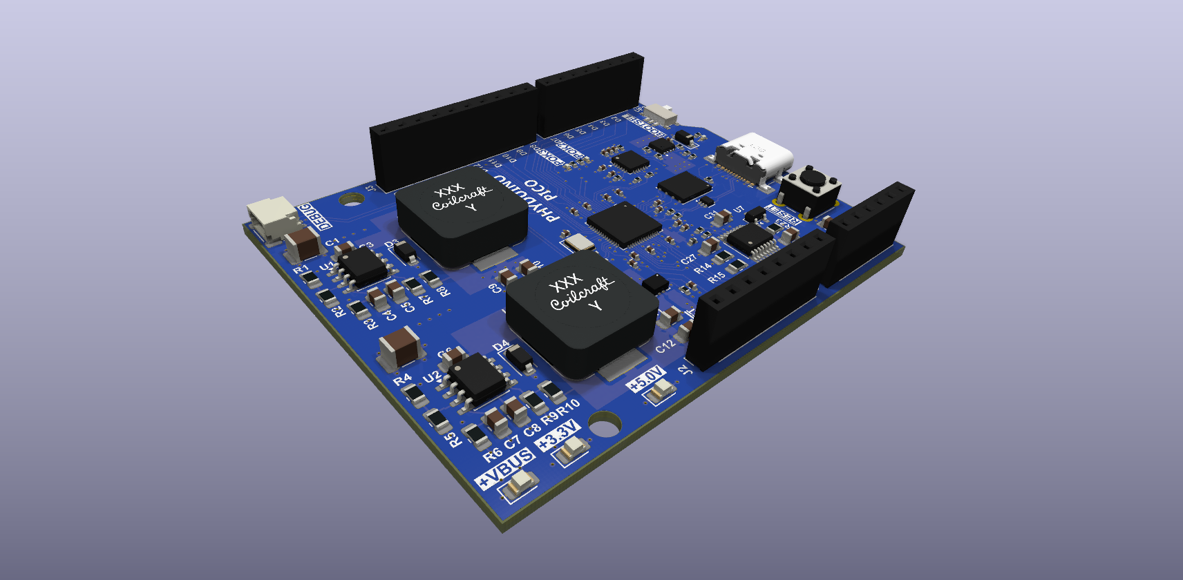
FQBN phyduino:rp2:phyduino_pico. Hardware design: ../phyduino_pico (KiCad, rev D/E).
| MCU | RP2040 (U4), 125 MHz | |
| Flash | W25Q128JV (U9), 16 MB; boot stage 2 = SDK W25Q080 (works for the whole W25Q family) | |
| Crystal | 12 MHz (Y1) | |
| LED | GPIO5, active high (LED_BUILTIN, Arduino pin 22) | |
| Boot mode | Slide switch SW1: 3.3 V = normal, GND = BOOTSEL (UF2 drive). No BOOTSEL button. | |
| Reset | SW2 (also header power pin 3) | |
| Debug | J1, 3-pin JST-SH SWD |
The authoritative table is the comment at the top of platform/variants/phyduino_pico/pins_arduino.h. Summary:
| Arduino pin | Header | RP2040 | Notes | |
|---|---|---|---|---|
| 0 / 1 | D0 RX / D1 TX | GPIO1 / GPIO0 | Serial1 (UART0) | |
| 2–9 | D2–D9 | GPIO6,7,8,9,10,15,16,17 | D4/D5 = Serial2 (UART1) | |
| 10–13 | D10 SS, D11 MOSI, D12 MISO, D13 SCK | GPIO13, 11, 12, 14 | SPI (SPI1) | |
| 14–16 | A0–A2 | GPIO26–28 | RP2040 ADC, 3.3 V full scale; also usable as digital pins | |
| 17–19 | A3–A5 | — | MAX11635 ADC, 2.048 V full scale, analog only | |
| 20 / 21 | SDA / SCL | GPIO24 / GPIO25 | Wire (I2C0); silkscreen D18/D19 | |
| 22 | (LED) | GPIO5 | LED_BUILTIN |
Numbering follows the Uno (A0–A5 = 14–19, so for (p = A0; p <= A5; p++) works). The silkscreen's D18/D19 names for SDA/SCL are not Arduino pin numbers here; use SDA/SCL (ADR 004).
| Chip | Bus / pins | Used by | |
|---|---|---|---|
| MAX11635 12-bit ADC (U5) | SPI0: SCK 22, MOSI 23, MISO 20, CS 21, EOC 19, CNVST 18 | analogRead(A3..A5) (ch 0–2); ch 3 = VBUS ÷ (100k/10.2k) | |
| LM4040 2.048 V reference (U7) | AREF header pin | MAX11635 reference only | |
| STUSB4500 USB-PD sink (U6) | I2C1: SDA 2, SCL 3, ALERT 4, RESET 29; address 0x28 | power profiles at start-up; #include <stusb4500.h> |
VBUS feeds the on-board regulator and the VIN pin, so VIN carries whatever voltage the USB-PD charger supplies. Tools > USB-PD Power (VIN) sets the highest voltage the board asks for; at start-up initVariant() loads the matching sink profiles into the STUSB4500 (variant.cpp). The 10 W limit (schematic) sets the current of the top profile:
| Menu option | Profiles | VIN on a USB-PD charger | |
|---|---|---|---|
| 5 V only (default) | 5 V/2 A | 5 V | |
| Up to 9 V | 5 V/2 A, 9 V/1 A | 9 V (POK2 lit) | |
| Up to 12 V | 5 V/2 A, 9 V/1 A, 12 V/0.83 A | 12 V, or 9 V if the charger has no 12 V (common) | |
| Up to 15 V | 5 V/2 A, 9 V/1 A, 15 V/0.66 A | 15 V (POK3 lit) | |
| Up to 20 V | 5 V/2 A, 9 V/1 A, 20 V/0.5 A | 20 V (POK3 lit) | |
| Use chip's stored settings (NVM) | left as loaded at power-up | 5 V on a Phyduino board |
An ordinary USB port always gives 5 V. A charger supplies the highest profile it can. The menu writes the chip's working registers only, never its NVM, and the board renegotiates only if they differ from what the chip already holds. A sketch can change them with stusb4500::setProfiles() and read the contract and measured VBUS (see stusb4500.h and tests/sketches/usbpd_status).
At plug-in, before any sketch runs (and during uploads), the chip negotiates from its NVM. ST's factory NVM asks for up to 20 V at 1 A, so Phyduino boards have their NVM set to 5 V only, once per board, with tests/sketches/usbpd_nvm (hardware checklist item 19). The NVM is good for about 1000 writes, which is why only that tool writes it.
The register addresses come from ST's register map, not the datasheet; tests/hardware-checklist.md item 14 checks them.
analogRead(), volts = reading * 3.3 / 1023 on A0–A2 but reading * 2.048 / 1023 on A3–A5. analogReference() does nothing.Wire enables the RP2040's weak internal pull-ups; use 4.7 kΩ to 3.3 V for longer wires or 400 kHz.Wire sets it.tone() on one changes the others' frequency. D1/D8, D0/D9, D6/A0, D11/A1 and D12/A2 are also the same channel, so they share the duty cycle too (table under analogWrite() in the API reference).phyduino_pico_bios sets it to i2c0 by mistake; this core uses I2C1. Wire (I2C0) is separate.millis(), delay(), USB, the ADCs and UART/SPI/I2C/PWM rates are unaffected. The fastest SPI clock is half the peripheral clock: CPU speed / 2 up to 133 MHz (66.5 MHz at the default), but 24 MHz above 133 MHz, where the peripherals run from the 48 MHz USB clock. The lowest tone()/PWM frequency scales with the clock: about 3 Hz at 50 MHz, 8 Hz at 133 MHz, 12 Hz at 200 MHz.-Os (default, smallest), -O2, -O3 (fastest) or -Og (for debugging) for the sketch, core and libraries.++/-- of a volatile variable (common in interrupt sketches); the code still works.setup1() and loop1() runs them on core 1 at the same time as setup()/loop() on core 0; rp2040.fifo passes values between them (arduino-pico compatible; API reference).setup()/loop() and setup1()/loop1() then run as tasks (API reference, ADR 009).